Intelligent Machines
Intel to Make Three-Dimensional Transistors
The company says the new architecture will result in better performance with less power.
Intel has shown off the design of its next generation of chips. The new transistor design, which uses a three-dimensional gate rather than a flat one, will go into production at the company’s fabs over the next year. The company says the three-dimensional structure will allow the company to double the density of its chips while also providing performance gains and lower power consumption. The design will first be rolled out in the company’s Core processor chips, used for desktops. After that they’ll be integrated into Intel’s mobile and handheld chip line, called Atom.
Intel says fabrication of the chip will be the first large-volume production of three-dimensional transistors. The new chips are 37 percent faster than the company’s current ones when operating at low voltages to keep power consumption low. And they require half the power to perform at a given switching speed. Power consumption is important in handheld devices because it determines how long the battery lasts. It’s also crucial in the power-hungry server farms that make up the cloud.
The best chips on the market today use planar transistors that are 32 nanometers in size. The next generation will use 22-nanometer transistors. To pack more processing power into that smaller size without sending power requirements through the roof, the company had to turn to a new design. “The difficulty in scaling the planar device was becoming extreme,” says William Holt, general manager of Intel’s technology and manufacturing group. The company’s 22-nanometer chips will be made entirely of three-dimensional transistors.
As they get smaller and smaller, conventional transistors are subject to a problem called leakage. This means that when the transistor is in the “off” state, a small amount of current still flows through. This leads to errors and drains power. Intel says the three-dimensional design is less subject to this problem.
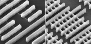
Conventional transistors use a metal electrode, called the gate, to control the flow of electrons through a planar channel in the silicon substrate. When the current applied by the gate is high enough, electrons flow through the channel between the source and drain electrodes. Intel’s three-dimensional design has these same basic elements. But instead of being flat, the channel is a raised “fin” of silicon surrounded on three sides by the gate. This allows for a more intimate connection between the gate and the channel, and that in turn enables better control, greatly reducing leakage. By connecting one set of electrodes to multiple “fins” in a single transistor, the company can make transistors that operate with a greater drive current—a plus for high-performance operation.
The company has been developing the tri-gate transistor since 2002. “The real challenge has been getting it ready for manufacturing,” says Mark Bohr, an Intel senior fellow. Bohr speculates that the company has a three-year lead over other chipmakers with this technology.
Intel says the production of the three-dimensional transistors won’t require any new manufacturing technologies. Extra etching steps will lead to a small production cost increase.
The company says the three-dimensional design will scale even further to the next generation of chips, which will use 14-nanometer transistors. Beyond that, it will need something new. “We’re really in an era where we can no longer shrink transistor sizes and expect significant benefits,” says Bohr. “We have to continually innovate and invent new structures and materials.”
