Intelligent Machines
Micro Chiplets
PARC’s technique of mincing chips into printer ink could revolutionize the way electronics are made.
In the same research lab where the ethernet, laser printer, and graphical user interface were born, engineers are forging an entirely new way to assemble electronic devices—a technique that could be faster, cheaper, and more versatile.
Typically, chips are made in bulk on semiconductor wafers and then cut into individual units and placed on motherboards inside computers and other devices. But researchers at PARC, in Palo Alto, California, envision doing something different with the wafers: chopping them up into hairs-width “chiplets,” mixing them into an ink, and guiding the tiny pieces electrostatically to just the right spot and orientation on a substrate, from which a roller could pick them up and print them.
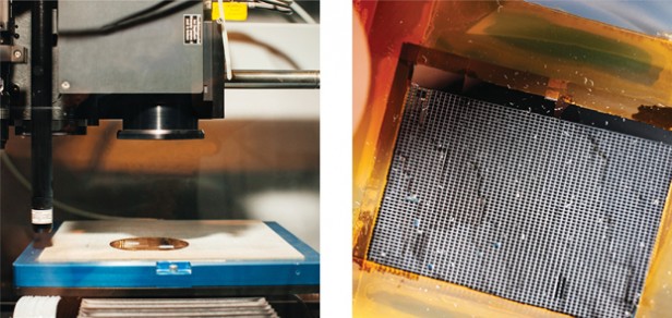
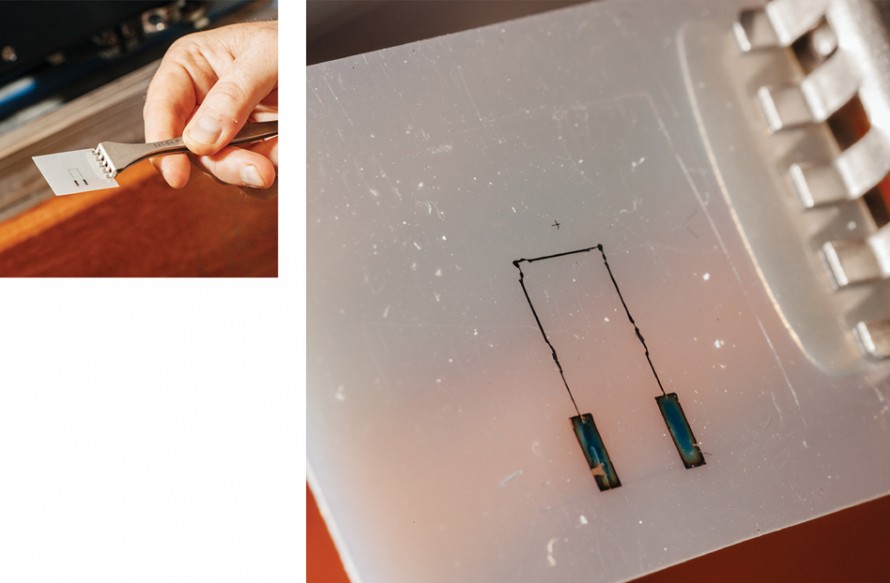
Right: The thousands of chiplets have positive and negative charges, applied to the wafer by way of thin films.

Although now at a very early stage, the technology could lead to novel kinds of computing devices, such as high-resolution imaging arrays made from tiny ultrasensitive detectors assembled by the million. Because printers can deposit materials on different substrates, this technology could be used to make high-performance flexible electronic devices, tiny sensors festooned with dense arrays of diverse sensors, or 3-D objects with computing functions woven in, says Janos Veres, who manages PARC’s printed-electronics team. And the approach could make it easier for more people and small companies to design and manufacture custom computing devices.
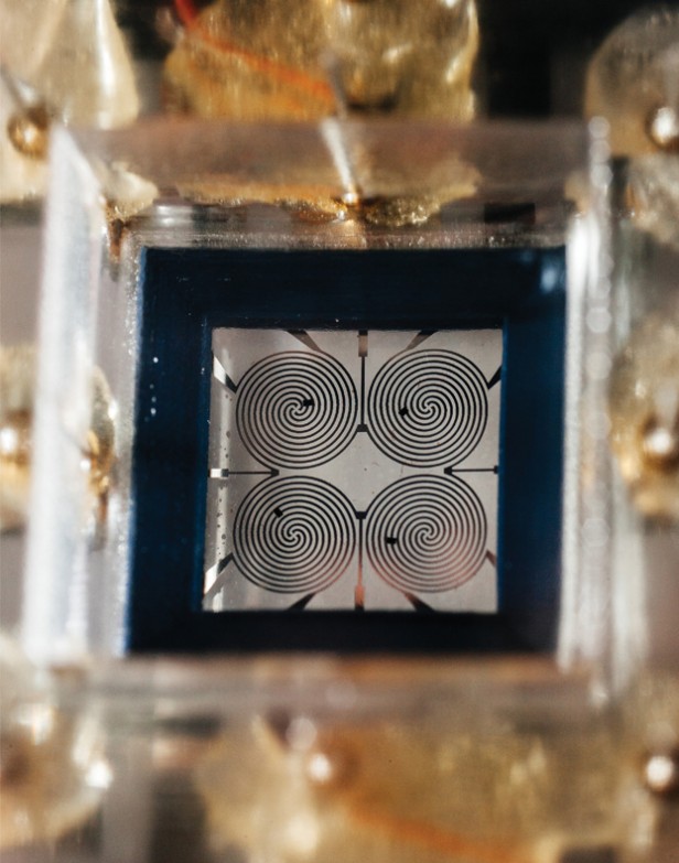
PARC’s vision for the technology starts with wafers made by conventional methods and designed to hold thousands of tiny functioning devices. These could include LEDs or lasers, processors and memory, or sensors based on microelectromechanical devices, or MEMS. They’d all become feedstocks for a palette of chip-infused inks. Existing electronics-printing systems generally use lower-performance materials, but “potentially, we can use the absolutely highest-performance chips on the market,” says Eugene Chow, an electrical engineer who leads the project.
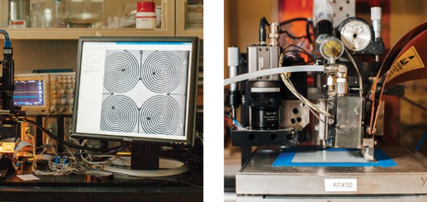
The technology marshals chiplets into place using software-controlled electrical fields generated by arrays of wires beneath an assembly substrate. Like balls rolling into divots, the chiplets go to locations defined by the electrical fields. “The fields are changing in time and space in all kinds of fancy patterns that can be controlled to allow high-throughput assembly,” Chow says.
For now, placement is aided by simple positive and negative charges added to chiplets before the wafers are minced. For a printing system to handle different kinds of chiplets, PARC envisions differentiating them with unique charge-based bar codes or creating multiple printing steps, with one type of chiplet set down at each step. “Years from now, if this works, it’s a new platform where we put millions and billions of things together,” Chow says.
The first hurdle is figuring out how to precisely assemble chiplets; so far, PARC has managed to place four at a time and then wire them together in a second step. Still, that achievement is a start toward “accelerating the evolution of microelectronics,” Veres says. “We can iterate new circuits every minute, opening up thousands of uses.”
