A Printing Process to Make Wall-Sized Displays
Researchers aim to print large areas of carbon nanotube thin-film transistors on plastic surfaces to make flexible displays and sensor networks.
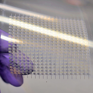
Adapting conventional printing technology, researchers have developed a way to rapidly and inexpensively make uniform arrays of high-performing transistors out of carbon nanotubes on flexible plastic sheets. The process could eventually lead to a tool for manufacturing large-area, low-power sensor arrays and displays.
Thin-film transistors made from carbon nanotubes are attractive for these types of applications because they are robust and mechanically flexible, and they can be much more energy efficient than silicon transistors. They can also be applied as a solution, or “ink,” and can be processed at relatively low temperatures, making them compatible with plastic substrates.
Researchers using techniques more like those used in conventional integrated-circuit fabrication have previously made prototypes of nanotube transistor arrays on flexible plastic, including responsive sensor networks called “electronic skin” (see “Electronic ‘Skin’ Emits Light When Pressed”). Carbon nanotube transistors have also been printed before, but their performance has lagged for one reason or another, says Ali Javey, a professor of electrical engineering and computer science at the University of California, Berkeley. Javey led the new work, which he says is the first demonstration of fully printed carbon nanotube transistor arrays that also consistently show very high performance—an important step toward roll-to-roll manufacturing of such devices.
In a paper published earlier this month in Nano Letters, Javey and his colleagues report using their multistep process to produce transistor arrays with much higher electron mobility than printed carbon nanotube transistors demonstrated previously.
Higher mobility makes the transistors more efficient and is crucial for displays, says Javey, because it means less voltage is required to supply the current necessary for running organic light-emitting diodes (OLEDs). The method his group has demonstrated “holds a lot of promise for very large-area displays—covering an entire wall with a display or a sensor array, for example,” he says. “If you are dealing with such large areas, in terms of manufacturing cost it’s just not feasible to use conventional-based processing.”
Javey uses a lab version of a well-known manufacturing process called gravure printing. In his setup, the plastic substrate is mounted to a cylindrical drum, which rolls it over a flat surface that serves as a mask, patterned with holes filled with inks made of the desired materials. In a roll-to-roll setup, a second roll would serve as the mask.
For now, Javey’s group will focus on refining this gravure method to further improve transistor performance and make the arrays more uniform. Eventually, the researchers hope to print more complicated integrated circuits that would include sensors and display components.
